
Jagran Josh
Semiconductors Formulas & Diagrams: Students can find a list of important diagrams and formulas for CBSE Class 12 Physics Chapter 13, Semiconductors. Use the PDF download link attached below to save the formula sheet.
CBSE Class 12 Physics Semiconductors Formulas: Central Board of Secondary Education is all set to conduct its upcoming board examinations in 2024. It has released all the important resources required for students to prepare for the Board Exams. As per the latest CBSE guidelines and updated Sample Paper 2024, multiple-choice questions have been added as a form of assessment in the question paper, which requires a lot of practice. Thus, in order to make this preparation easy and quicker, students should either prepare a formula sheet of their own or refer to the formula sheet presented here.
This formula sheet consists of all the formulas from Class 12 Physics Part 2 Chapter 13, Semiconductors. Along with the formulas, we have also included all the important definitions and diagrams for you to practise and remember. We have also attached a PDF download link below which can be saved by students and used as per their convenience. Along with practice for Board Examinations, this formula sheet will come in handy in preparation for competitive exams such as JEE and NEET.
It is advisable for students to refer to the formula sheet presented here if they want to save their time and effort in searching for formulas while solving questions and answers or practising frequently. Since physics is a subject filled with lots of diagrams and formulas, it is important that formula sheets for such subjects should be prepared. Chemistry, Mathematics, and Accountancy are some subjects for which students should prepare formula sheets or refer to it.
Related:
Formulas:
- Resistivity (ρ)= 1/Conductivity(σ)
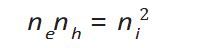
- Intrinsic carrier concentration (Ni)= number of free electrons (Ne) = number of holes (Nh)
- Total current (I) = electron current (Ie) + hole current (Ih)
- Electron and hole concentration in thermal equilibrium=
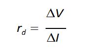
- Dynamic Resistance=
Definitions:
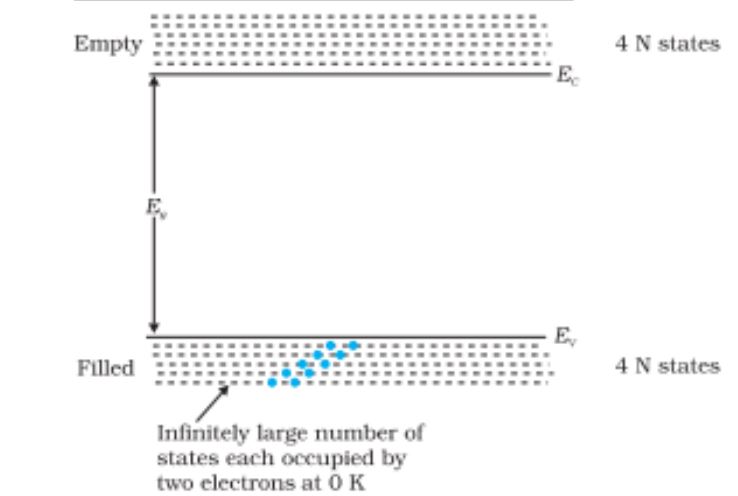
Energy Bands– Different energy levels with continuous energy variation form are called energy bands
Valence Band– The energy band which includes the energy levels of the valence electrons is called the valence band
Conduction Band– The energy band above the valence band is called the conduction band.
Energy Band Gap – The gap between the top of the valence band and the bottom of the conduction band is called the energy band gap.
Valence bond/covalent bond- These shared electron pairs are referred to as forming a covalent bond or simply a valence bond.
Extrinsic Semiconductors– When a small amount, say, a few parts per million (ppm), of a suitable impurity, is added to the pure semiconductor, the conductivity of the semiconductor is increased manifold. Such materials are known as extrinsic semiconductors or impurity semiconductors. They are also known as impurity semiconductors.
Doping- The deliberate addition of a desirable impurity is called doping.
Dopants– The deliberate addition of the impurity atoms are called dopants.
n-type semiconductors– In an extrinsic semiconductor doped with pentavalent impurity, electrons become the majority carriers and holes the minority carriers. These semiconductors are, therefore, known as n-type semiconductors. For n-type semiconductors. Ne>>Nh.
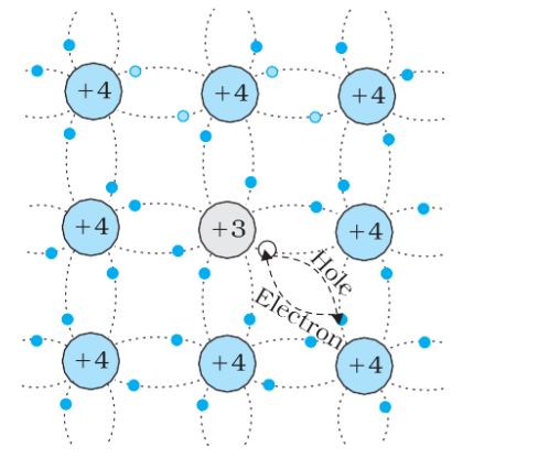
p-type semiconductors– extrinsic semiconductors doped with trivalent impurity are called p-type semiconductors. Nh>>Ne.
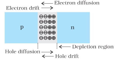
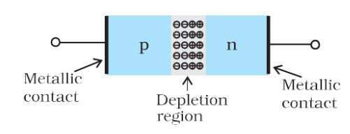
Depletion Region– When a hole diffuses from p ® n due to the concentration gradient, it leaves behind an ionized acceptor (negative charge) which is immobile. As the holes continue to diffuse, a layer of negative charge (or negative space-charge region) on the p-side of the junction is developed. This space-charge region on either side of the junction together is known as the depletion region.
Drift– The motion of charge carriers due to the electric field is called drift.
Barrier Potential– The potential that tends to prevent the movement of electrons from the n region into the p region, it is often called a barrier potential.
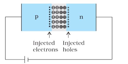
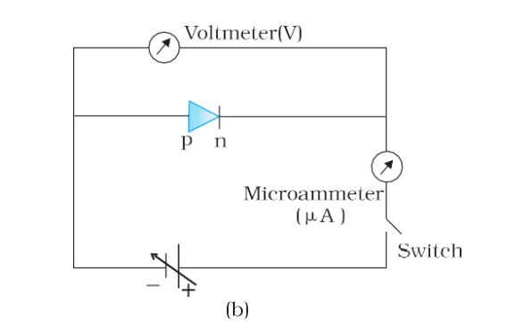
Forward Biased– When an external voltage V is applied across a semiconductor diode such that the p-side is connected to the positive terminal of the battery and the n-side to the negative terminal, it is said to be forward-biased.
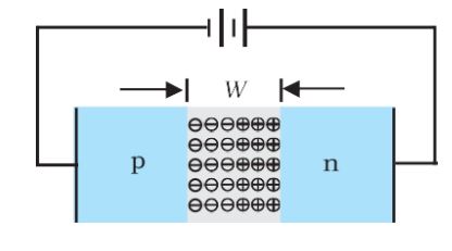
Reverse Biased– When an external voltage (V ) is applied across the diode such that the n-side is positive and the p-side is negative, it is said to be reverse-biased
Breakdown Voltage– The current under reverse bias is essentially voltage independent up to a critical reverse bias voltage, known as breakdown voltage.
Threshold voltage/Cut-in Voltage– After the characteristic voltage, the diode current increases significantly (exponentially), even for a very small increase in the diode bias voltage. This voltage is called the threshold voltage or cut-in voltage.
Reverse Saturation Current– For the diode in reverse bias, the current is very small (~mA) and almost remains constant with change in bias. It is called reverse saturation current.
Rectifier– The device is used to rectify alternating voltages and the circuit used for this purpose is called a rectifier.
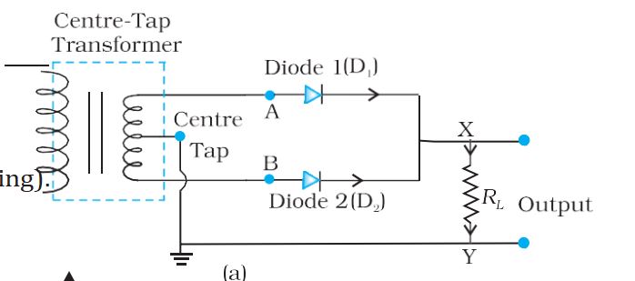
Full-wave rectifier- The circuit using two diodes, shown in Fig. 14.19(a), gives output rectified voltage corresponding to both the positive as well as negative half of the ac cycle. Hence, it is known as a full-wave rectifier.
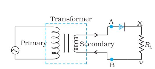
Half-wave rectifier– Since the rectified output of this circuit is only for half of the input ac wave it is called as half-wave rectifier.
Centre tap transformer– For a full-wave rectifier the secondary of the transformer is provided with a centre tapping and so it is called centre-tap transformer.
Diagrams:
Showcase of energy bands
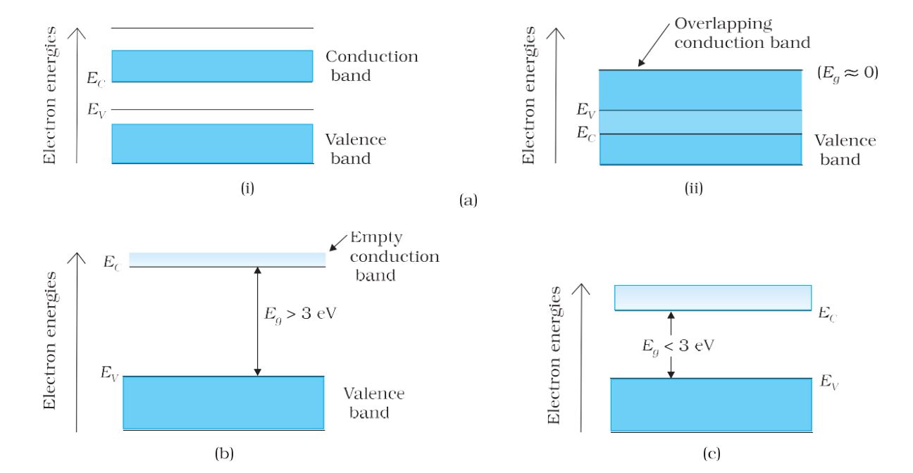
Difference between energy bands of metals, semiconductors, and insulators
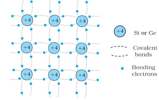
Schematic 2D diagram of Si or Ge structure
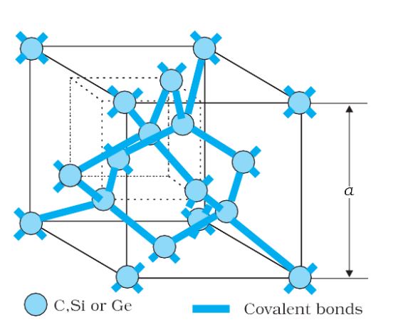
3D Diagram of Si or Ge structure
Pentavalent donor

Trivalent acceptor
P-n junction
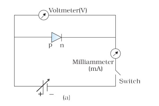
Semiconductor Diode
Symbol for p-n junction diode
![]()
Forward Biased
Reverse Biased
Circuit arrangement in forward-biased
Circuit arrangement in reverse-biased
Half-wave rectifier
Full-wave rectifier
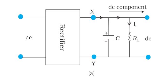
Full-wave rectifier with capacitor filter
To download the formula sheet in PDF, click on the link below
Also Find:
#CBSE #Class #Physics #Semiconductors #Formula #List #Definitions #Diagrams